AntiLog amplifier or anti–logarithmic amplifier is an electronic circuit that produces output that is proportional to the anti-logarithm of the applied input. Basically it performs mathematical operation of an anti-logarithm. In this article, we will see the different antilog amplifier circuits, its working and antilog amplifier applications. Basically two circuits are there to perform the anti-logarithmic function. First, using diode and op-amp and second, using BJT and op-amp.
Antilog amplifier using diode and op-amp
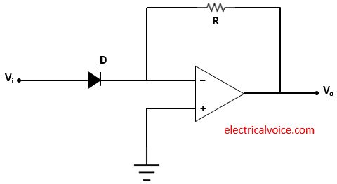
Diode, resistor and op-amp used in the antilog amplifier as shown in figure 1. The input Vi is applied through diode D at the inverting terminal. Vo is the output voltage. The non-inverting terminal of the op-amp is connected to the ground. This means that the voltage of the non-inverting terminal is zero volts.
Analysis
The analysis of the antilog amplifier is shown in figure 2. Since the op-amp is ideal and negative feedback is present, the voltage of the inverting terminal (V−) is equal to the voltage of the non-inverting terminal (V+ = 0V), according to the virtual short concept.
V− = V+ = 0V
The currents entering both terminals of the op-amp are zero since the op-amp is ideal.
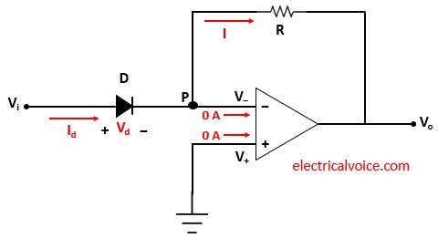
Let current I flows through the resistor R.
\begin{equation} \label{eq:poly}
I=\frac{0-V_{o}}{R}=-\frac{V_{o}}{R}
\end{equation}
and diode current $I_{d}$,
\begin{equation} \label{eq:poly}
I_{d}=I_{o}e^{\frac{V_{d}}{\eta V_{T}}}
\end{equation}
where $V_d$ = forward bias voltage across diode D
Apply KCL at node P
$I_{d} = 0 + I$
\begin{equation} \label{eq:poly}
I = I_{d}
\end{equation}
and
$V_{d} = V_{i}-0$
\[V_{d} = V_{i}\]
Therefore, equation (2) becomes
\begin{equation} \label{eq:poly}
I_{d}=I_{o}e^{\frac{V_{i}}{\eta V_{T}}}
\end{equation}
From equation (1), (3) and (4), we have
\[-\frac{V_{o}}{R}=I_{o}e^{\frac{V_{i}}{\eta V_{T}}}\]
Therefore, we have
\[
\quicklatex{color=”#000000″ size=20}
\boxed{V_{o}=-I_{o}Re^{\frac{V_{i}}{\eta V_{T}}}}
\]
Note: The negative sign in the output signifies that there is a 180° phase difference between output and the applied input.
Antilog amplifier using diode and transistor
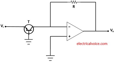
Another circuit comprises of a BJT (PNP) T, resistor (R) and op-amp used as the antilog amplifier as shown in figure 3. The input Vi is applied through transistor T at the inverting terminal. Vo is the output voltage. The non-inverting terminal of the op-amp is connected to the ground. This means that the voltage of the non-inverting terminal is zero volts.
Analysis
The analysis of the antilog amplifier is shown in figure 4. Since the op-amp is ideal and negative feedback is present, the voltage of the inverting terminal (V−) is equal to the voltage of the non-inverting terminal (V+ = 0V), according to the virtual short concept.
V− = V+ = 0V
The currents entering both terminals of the op-amp are zero since the op-amp is ideal.
Let current I flows through the resistor R.
\begin{equation} \label{eq:poly}
I=\frac{0-V_{o}}{R}=-\frac{V_{o}}{R}
\end{equation}
and collector current $I_{C}$,
\begin{equation} \label{eq:poly}
I_{C}=I_{s}e^{\frac{V_{EB}}{\eta V_{T}}}
\end{equation}
where $V_{EB} = V_E – V_B$
and Is = Reverse saturation current of emitter-base junction
As we know that
$I_C + I_B = I_E$
since IB ≅ 0 A
Therefore
\begin{equation} \label{eq:poly}
$I_C = I_E$
\end{equation}
Apply KCL at node P
$I_E = 0 + I$
\begin{equation} \label{eq:poly}
I = I_{E}
\end{equation}
and
$V_{EB} = V_{i}-0$
\[V_{EB} = V_{i}\]
Therefore, equation (6) becomes
\begin{equation} \label{eq:poly}
I_{C}=I_{s}e^{\frac{V_{i}}{\eta V_{T}}}
\end{equation}
From equation (5), (7), (8) and (9), we have
\[-\frac{V_{o}}{R}=I_{s}e^{\frac{V_{i}}{\eta V_{T}}}\]
Therefore, we have
\[
\quicklatex{color=”#000000″ size=20}
\boxed{V_{o}=-I_{s}Re^{\frac{V_{i}}{\eta V_{T}}}}
\]
Note: The negative sign in the output signifies that there is a 180° phase difference between output and the applied input.
Antilog Amplifier Applications
1. It is used in analog multiplier circuits.
