OR gate is a device which has two or more inputs and one output. The output of an OR gate is logical 1 (high) only if one or more inputs are logical 1 (high). In Boolean algebra, the term OR is represented by plus (+) and the Boolean expression Y = A+B indicates Y equals A or B.
OR gate Symbol
The OR gate logic symbol is shown in figure 1.

OR gate Truth table
The OR gate truth table is given below.
| A | B | Y = A+B |
| 0 | 0 | 0 |
| 0 | 1 | 1 |
| 1 | 0 | 1 |
| 1 | 1 | 1 |
OR gate Circuit Diagram
The OR gate can be realised by the electronic circuit by using two ideal p-n junction diodes D1 and D2 as shown in fig. 2.
Here negative terminal of the battery is grounded and corresponds to the logical 0 (low) and positive terminal of the battery (i.e. voltage 5 V in the present case) corresponds to logical 1 (high). One terminal of resistance R1 is grounded. The output voltage is Y w.r.t. ground. The operation of OR gate can be understood by the following four cases.
Case-1: When both A and B are connected to earth (i.e. A = 0 and B = 0)
In this case, none of the diodes will conduct and therefore no voltage develops across resistance R. The output voltage is zero w.r.t.earth. Hence the output Y is at logical 0.
Case-2: When A is earthed and B is connected to positive terminal of battery of 5 V (i.e. A = 0 and B = 1)
In this case, the diode D2 will conduct while D1 will not conduct. Since D2 is ideal, no voltage drop takes place across D2. Therefore, a voltage drop of 5 V takes place across R, having Y at 5 volt w.r.t. earth. Now the output Y is at logical 1.
Case-3: When A is connected to positive terminal of battery of 5 V and B is earthed (i.e. A = 1 and B = 0)
In this case, the diode D1 will conduct while D2 will not conduct. Since diode D1 is ideal, no voltage drop takes place across D1. Therefore, a voltage drop of 5 V takes place across R, having Y at 5 volt w.r.t. earth. Now the output Y is at logical 1.
Case-4: When A and B both are connected to positive terminal of battery of 5 V (i.e. A = 1 and B = 1)
In this case, both the diodes D1 and D2 get forward biased and hence conduct. Since the diodes are ideal and connected in parallel, the voltage drop across R cannot excess 5 V. Therefore, a voltage drop of 5 V takes place across R, with Y at 5 V potential w.r.t. earth. Thus the output Y is at logical 1.
Hence it can be concluded that the output of an OR gate is at logical 1 only if one or more inputs are at logical 1.
Switch Circuit of OR gate
The switch circuit having function similar to the OR gate is shown in figure 3.
In this arrangement, Switch OFF (or open) corresponds to logical 0 and switch ON (or closed) corresponds to logical 1. The inputs are introduced through the switch S1 and S2. The lighting of the bulb L is the output. Here, we find that the bulb glows (i.e. output is 1) when either switch S1 is closed or S2 is closed or both the switches are closed. The bulb remains off (i.e. output is 0) only when both the switches are open (i.e. A = 0, B = 0).
OR gate using NAND gate
To produce OR gate using NAND gate, the inputs A and B of the two NOT gates (obtained from the NAND gates) are joined together. The inputs A and B will get inverted. These outputs are then fed as inputs to the NAND gate as shown in fig. 4.
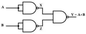
The truth table of the above combination is given below.
| A | B | X | Z | Y = A+B |
| 0 | 0 | 1 | 1 | 0 |
| 0 | 1 | 1 | 0 | 1 |
| 1 | 0 | 0 | 1 | 1 |
| 1 | 1 | 0 | 0 | 1 |
OR gate using NOR gate
To produce OR gate using NOR gate, the output of the NOR gate is fed as input to NOT gate (made from NOR gate by joining the two inputs) as shown in fig. 5.
The truth table of the above combination is given below.
| A | B | X | Y = A+B |
| 0 | 0 | 1 | 0 |
| 0 | 1 | 0 | 1 |
| 1 | 0 | 0 | 1 |
| 1 | 1 | 0 | 1 |
