A NAND gate is a combination of an AND gate and NOT gate. If we connect the output of AND gate to the input of a NOT gate, the gate so obtained is known as NAND gate. This gate is also called as Negated AND gate.
In Boolean expression, the NAND gate is expressed as![]() and is being read as “A and B negated” or “A and B bar”.
and is being read as “A and B negated” or “A and B bar”.
NAND gate symbol
The logic symbol of NAND gate is shown in figure 1(a).
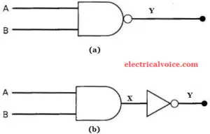
Figure 1(b) shows the NAND gate as the combination of AND gate and NOT gate.
NAND gate truth table
The NAND gate truth table for figure 1(a) is shown below.
| A | B | |
| 0 | 0 | 1 |
| 0 | 1 | 1 |
| 1 | 0 | 1 |
| 1 | 1 | 0 |
The NAND gate truth table for figure 1(b) is shown below.
| A | B | X = A.B | |
| 0 | 0 | 0 | 1 |
| 0 | 1 | 0 | 1 |
| 1 | 0 | 0 | 1 |
| 1 | 1 | 1 | 0 |
From NAND gate truth table, it can be concluded that the output will be logical 0 or low when all inputs are at logical 1 or high.
NAND gate as Universal gate
A universal gate is a gate which can implement any Boolean function without need to use any other gate type. The NAND and NOR gates are universal gates.
The repeated use of the NAND gate can produce all other logic gates. Thus in digital circuits, it serves as a building block.
NOT gate using NAND gate
If the two inputs of the NAND gate are joined to make one input as shown in figure 2 below then the NAND gate functions as a NOT gate. In the truth table of NAND gate, if we use B = A, we obtain the truth table of NOT gate.
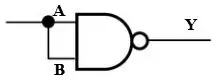
The truth table of the above combination is given below.
| A | B = A | Y |
| 0 | 0 | 1 |
| 1 | 1 | 0 |
OR gate using NAND gate
To produce OR gate using NAND gate, the inputs A and B of the two NOT gates (obtained from the NAND gates) are joined together. The inputs A and B will get inverted. These outputs are then fed as inputs to the NAND gate as shown in fig. 3.
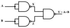
The truth table of the above combination is given below.
| A | B | X | Z | Y = A+B |
| 0 | 0 | 1 | 1 | 0 |
| 0 | 1 | 1 | 0 | 1 |
| 1 | 0 | 0 | 1 | 1 |
| 1 | 1 | 0 | 0 | 1 |
AND gate using NAND gate
To produce AND gate using NAND gate, the output of the NAND gate is connected to the NOT gate (made from NAND gate by joining the two inputs) as shown in fig. 4.
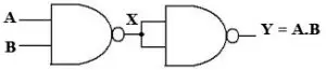
The truth table of the above combination is given below.
| A | B | X | Y = A.B |
| 0 | 0 | 1 | 0 |
| 0 | 1 | 1 | 0 |
| 1 | 0 | 1 | 0 |
| 1 | 1 | 0 | 1 |
Exercise
Q. Why are the NAND gates called as a digital building block?
Answer. The repeated use of NAND gates can produce all the three basic gates i.e. OR, AND, and NOT gates; whose various combinations provide us large number of complicated digital circuits. Hence in digital circuits, NAND gate is called as a digital building block.
Q. What do you mean by the truth table of a logic gate?
Answer. It is table which shows all the input/output possibilities for a logic gate.
Q. Name the types in which the electronic circuits have been classified.
Answer. The electronic circuits can be classified as (a) analog circuits and (b) digital circuits.
