The NOT gate is a device that has only one input and one output. It is a logic gate that inverts the input digital signal. That is why NOT gate is also known as Inverter.
In Boolean algebra, the term NOT is represented by bar symbol (‾) and the Boolean expression ![]() indicates that Y equals not A. The logical symbol of a NOT gate is figure 1.
indicates that Y equals not A. The logical symbol of a NOT gate is figure 1.

The operation of NOT gate is based on the following rule:
The output of a NOT gate is logical 1 (high) if input is logical 0 (low).
The output of a NOT gate is logical 0 (low) if input is logical 1 (high).
NOT gate Truth table
| Input (A) | Output (Y = |
| 0 | 1 |
| 1 | 0 |
Switch Circuit of NOT gate
The switch circuit having function similar to the NOT gate is shown in figure 2. In this arrangement switch OFF (or open) corresponds to logical 0 and switch ON (or closed) corresponds to logical 1.
The input is introduced through the switch A. The lighting of the bulb Y is output. The bulb glows (i.e. output is 1) only when switch A is OFF (i.e. A = 0) and bulb does not glow (i.e. output is 0) when switch A is closed (i.e. A = 1).
Realization of NOT Gate
A NOT gate cannot be realised by using diodes. However it can be realised by making use of a transistor. An electronic circuit of NOT gate using npn transistor is shown in figure 3.
The base of the npn transistor Q1 is connected to the input A through resistance R1 and the emitter is grounded. The collector is grounded through a resistor R2 and a 5 V battery. The output Y is the voltage with respect to earth. The operation of the NOT gate can be understood by the following two cases.
Case-1: When input A is grounded (i.e. A = 0), the base of the transistor Q1 also gets grounded. Now, base-emitter junction is not forward biased. On the other hand, base-collector junction is reversed biased. As the emitter current is zero, the base current is also zero and hence the collector current will also be zero. Under these conditions, the transistor Q1 is said to be in cut off mode and the output voltage Y will be +5 V w.r.t. earth. Hence the output Y voltage is +5 volts. Therefore, the output Y is at logical 1.
Case-2: When input A is connected to positive terminal of 5 V battery (i.e. A = 1), the base-emitter junction becomes forward biased. There will be emitter current, base current and collector current. The values of resistors R1 and R2 are so adjusted that in this arrangement, a large collector current flows. In this situation, the transistor is said to have gone to saturation mode. The voltage drop across R2 due to forward biasing of emitter is just equal to 5 V, which is equal and opposite to the potential drop across R2 due to battery in collector circuit. Hence the output Y voltage is zero volts. Therefore, the output Y is at logical 0.
NOT gate using NAND gate
If the two inputs of the NAND gate are joined to make one input as shown in figure below then the NAND gate functions as a NOT gate. In the truth table of NAND gate, if we use B = A, we obtain the truth table of NOT gate.
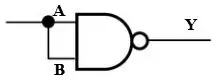
| A | B = A | Y |
| 0 | 0 | 1 |
| 1 | 1 | 0 |
NOT gate using NOR gate
To produce NOT gate using NOR gate, the two inputs are joined together as shown in figure 4.
The truth table of the above combination is given below.
| Input (A) | Output (Y = |
| 0 | 1 |
| 1 | 0 |
Exercise
Q. State the rule used in the operation of NOT gate?
Answer. The output of NOT gate is logical 1 if input is logical 0 and vice versa.
Q. Discuss how a NOT gate is realized using NAND gate.
or
Explain how the NOT gate can be obtained from the NAND gate?
Answer. If the two inputs of the NAND gate are joined to make one input as shown in figure below then the NAND gate functions as a NOT gate. In the truth table of NAND gate, if we use B = A, we obtain the truth table of NOT gate.
| A | B = A | Y |
| 0 | 0 | 1 |
| 1 | 1 | 0 |
Q. Mention the names of three basic logic gates.
Answer. The basic logic gates are
- OR gate
- AND gate
- NOT gate
