For the normal working of Silicon controlled rectifier (SCR), the operating conditions should not exceed SCR’s specified ratings. But practically, the SCR may be subjected to abnormal conditions such as overvoltages, overcurrent, high dv/dt, high dI/dt and excessive heating. This may lead to the SCR to work abnormally and may cause unwanted turn-on or permanent destruction. So in this article, we will see various thyristor protection or SCR Protection schemes which ensure reliable and satisfactory operation of thyristors.
There are five different types of SCR protection schemes available.
1. Overvoltage protection
2. Overcurrent protection
3. dv/dt protection
4. dI/dt protection
5. Thermal protection
Overvoltage protection
Overvoltage is of two types
1. External overvoltage
2. Internal overvoltage
External overvoltage
These are caused due to interruption of the flow of the current in the supply system or transmission line which is feeding the SCR or it is due to the lightening strokes caused in the transmission line feeding the SCR. Hence we need protection against external overvoltages.
Internal overvoltage
The large voltage may be produced internally within the SCR after the commutation process. A reverse recovery current decays abruptly with high di/dt which causes a high reverse voltage. As, V = L(di/dt) so if di/dt is high then V will be large and if such kind of heavy voltage exceed the breakdown voltage (VBO) of the SCR, SCR get false triggered and may get damaged. Hence we need protection against internal overvoltages.
Consider the following circuit. Assuming the gate signal is zero.
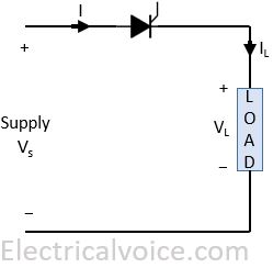
VSCR(specified) = voltage rating of SCR
If Vs > VSCR(specified)
then SCR may get false triggered and may get damaged.
If Vs < VSCR(specified)
then SCR will not be triggered until the gate signal is applied and SCR is safe.
Protective Measure
A non-linear resistor i.e. VARISTOR is used for protection against overvoltage. In power electronics, it is preferred to use Metal oxide silicon (MOS) type VARISTOR.
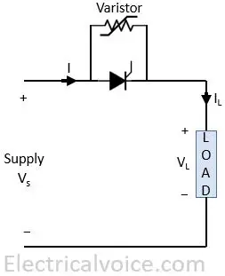
If Vs > VSCR(specified)
then resistance of varistor will become low and current will pass through it. Hence SCR will be safe.
If Vs < VSCR(specified)
then resistance of varistor will become high and SCR may get triggered by the gate signal.
Overcurrent Protection
If SCR is subjected to overcurrent (due to fault current or surge current or short circuit current) then SCR may get damaged because the junction temperature of the SCR may get increased at a very high rate and the heating effect will be very high. Hence it may cause permanent damage to the SCR.

ISCR(specified) = current rating of SCR
If I > ISCR(specified)
then SCR may get damaged permanently due to excessive heating at the junction.
If I < ISCR(specified)
then SCR will be safe.
Protective Measure
For the protection against overcurrent, fuses or circuit breaker may be used. Figure 4 shows the use of FACLF for SCR overcurrent protection. FACLF stands for fast-acting current-limiting fuse.
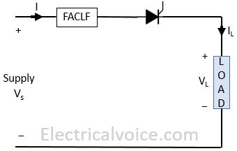
Note: While using the protection against overcurrent, the heat must be constant while designing the fuse for this purpose. It means that I2t product must be constant. Here I is the current flowing through the fuse or SCR and t is the time duration. So to protect the SCR, (I2t) rating of the fuse must be less than (I2t) rating of SCR.
I2t = constant
I12t1 = I22t2 = I32t3 = ….. = In2tn = constant
The SCR to be protected,
(I2t)rating(fuse) < (I2t)rating(SCR)
or
(I)rating(fuse) < (I)rating(SCR)
dI/dt protection
The current through the SCR can not be allowed to increase very fast as SCR will develop hotspots and may damage.

then SCR is safe

then SCR may get damage. Hence it needs protection against high dI/dt.
Protective Measure
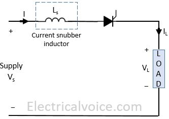
To limit the very high value of dI/dt, an inductor (Ls) is used in the circuit in series with the SCR. This inductor (Ls) is known as current snubber inductor or dI/dt inductor.
dv/dt protection
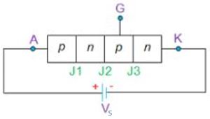
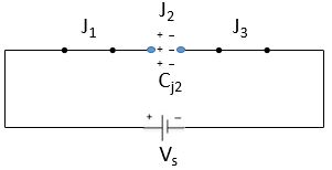
Consider the SCR in forward blocking mode as shown in figure 6. The junction J1 and J3 will be forward biased and junction J2 will reverse biased. This junction J2 behave as a capacitor (having capacitance Cj2) due to charge existing across the junction as shown in figure 7. A charging current, Icharging, will flow through the SCR. If V is the voltage across the junction J2 then charging current is given as
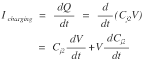
Cj2 is constant, hence

As the dV/dt increases, charging current increases. From the above discussion, it can be concluded that
If Icharging > Ilatching
then SCR will be triggered and SCR will be ON.
If Icharging < Ilatching
then SCR will be in forward blocking mode and hence OFF.
If the rate of rise of the anode to cathode voltage is high, charging current through the junction J2 capacitor may be sufficient to turn-on the SCR. This unwanted turn-on may occur due to noise signals (spurious spike of voltage caused due to other equipment). A high value of charging current may also damage the SCR. The SCR must be protected against the maximum permissible dv/dt of the SCR as specified by the manufacturer.

then SCR will not be triggered.

then SCR is false triggered. Hence it needs protection against high dv/dt.
Protective Measure
To prevent the unwanted turn-on of the SCR due to large dv/dt, a voltage snubber circuit can be used in parallel with the SCR.

Thermal protection
There are a number of losses associated with SCR working. These losses are as follows
- Conduction losses (during forward conduction mode)
- switching losses (during turn-on and turn-off process)
- losses associated with leakage current (during forward blocking mode or reverse blocking mode)
- gate circuit losses (due to the flow of gate current)
The temperature of the SCR may exceed the allowable temperature rating of the SCR due to above losses and SCR may get damaged. Hence SCR needs protection against this situation.
Protective Measure
To protect SCR from high temperature, SCR’s are assembled on heat sinks. To get best results heat sinks are generally made up of aluminium.
Before designing the heat sink, first of all, see the electrical and thermal analogy.
| S.No. | Electrical quantity | Thermal quantity |
| 1. | Charge (coulomb) | Heat (Joule) |
| 2. | Potential difference (volt) | Temperature difference (degree centigrade or °C) |
| 3. | Rate of flow of charge
or Current (ampere) |
Rate of flow of heat
or Thermal power (watt) |
| 4. | Electrical resistance (ohm or volt/ampere) | Thermal resistance (°C/watt) |
Consider the following diagram.
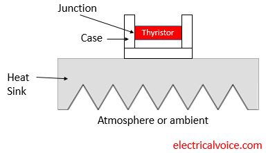
Tj = junction temperature
Tc = case temperature
Ts = sink temperature
Ta = atmospheric or ambient temperature
Tj > Tc > Ts > Ta
The heat flow is as follows
junction → case → sink → atmosphere (or ambient).
By using the above electrical analogy, the thermal equivalent circuit for thyristor (or SCR) is shown in figure 10.
θjc = thermal resistance from junction to case
θcs = thermal resistance from case to heat sink
θsa = thermal resistance from the heat sink to the atmosphere
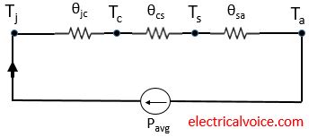
The average rate of heat generated by thyristor junction Pavg can be found out from the above circuit.

